


Appendix 1
The MOS Silicon-Gate Technology
MOS integrated circuits
In 1967, the MOS technology allowed us to realize the same logic functions made with bipolar technology using from five to 10 times less silicon area and from five to 10 times less power dissipation. However, the speed of MOS ICs was about fifty times slower, greatly limiting their possible applications. Almost all the experts thought that MOS ICs were too slow and too unreliable to ever challenge the dominance of bipolar technology.
The MOS technology in production used P-channel transistors with aluminum gates and a threshold voltage ranging from -4 to -8 volts. The supply voltage was -24 volts. Only RCA in the United States had developed an expensive CMOS (complementary MOS) manufacturing process primarily used for mobile military applications.
To avoid any interference between the various transistors of an integrated circuit, it was essential to hold the threshold voltage of the parasitic MOS transistors1 below the supply voltage. This requirement was met by using a sufficiently thick field oxide. However, the oxide thickness could not be arbitrarily large since the aluminum lines crossing over oxide steps would thin down at the step and could break if the oxide thickness exceeded a certain value.2 Thus, MOS technology required a delicate balance between conflicting requirements, providing only a small margin of safety.
The other major limitation was the high parasitic capacitance between the gate electrode and the source and drain of the transistor, due to the necessary alignment tolerances of the gate mask with respect to the source-and-drain mask (Fig. A2). The most damaging parasitic capacitance was Cgd, the overlap capacitance between the gate and the drain, due to the Miller effect.
The total input capacitance of a transistor in a circuit is equal to CG + Cgs + A·Cgd, where CG is the active capacitance of the MOS channel, Cgs is the parasitic overlap capacitance between the gate and the source, and A is the gain of the circuit of which the transistor is part (A·Cgd represents the Miller effect).
Since the gain A is generally much greater than 1 during the switching of the circuit, the impact of Cgd on the switching speed of the transistor is considerable. Moreover, the variability of Cgd due to all possible mask misalignments is very large, causing a broad wafer-to-wafer distribution of the speed of the integrated circuits (ICs).
The ideal process for MOS circuits was recognized by most insiders as early as 1966. It consisted of using wafers with [100] crystal orientation instead of [111] because the threshold voltage could be lowered to be in the range of -2 to -4 volts, allowing the supply voltage to be reduced from -24 to -15 volt. This change would also reduce the power dissipation by about a factor of two. Unfortunately, using [100] wafers, the field threshold voltage would be lower than the supply voltage for the maximum permissible oxide thickness. And this problem prevented using the low-threshold-voltage technology.
In 1966, Robert Bower realized that if the gate electrode had been defined first, the boundaries of the channel between the source and the drain would be determined by a single mask, thus avoiding the excessive and variable parasitic capacitances due to the misalignment between the first two masks. Bower's method consisted of using aluminum as a mask to define the source and drain regions. However, since aluminum does not withstand the high temperature required for thermal doping, Bower proposed using ion implantation, a novel invention that allowed low-temperature doping and was under development at Hughes Aircraft where Bower worked.
Bower's idea, however, worked only in principle but not in practice, because during the ion bombardment, the silicon lattice would be altered. To restore it, it was necessary to subject the wafer to a thermal annealing process at temperatures higher than those bearable by the aluminum. A more refractory material than aluminum was needed.
The Bower process was described in U.S. Pat. 3,472,712 filed October 27, 1966 and published October 14, 1969 [2]. It was never used to produce integrated circuits as described in the patent and the details of the process were unknown before the date of publication.
In 1967, John Sarace and collaborators at Bell Labs fabricated the first discrete transistors with a self-aligned gate made of amorphous silicon [4]. Their experiment consisted of growing a thin oxide layer on a wafer, followed by vacuum deposition of amorphous silicon. The silicon was then masked in the form of a ring and therefore the drain was inside the ring and the source was in common with all the other transistors. This process allowed them to prove in the laboratory that MOS transistors with self- aligned silicon gates could be made. However, the transistors were not isolated and therefore integrated circuits could not be made.
Toward the end of 1967, Tom Klein measured the difference in working function between P+ doped amorphous silicon and monocrystalline N-doped silicon. He found that by using P+ doped silicon, the threshold voltage of a P-channel MOS transistor could be reduced by 1.1 volts compared with an identical aluminum-gate device. This was enough to make MOS transistors with low-threshold voltage using the same [111] silicon orientation employed for the high-threshold voltage process.
The overall process architecture that I independently invented at Fairchild was like the one described in Bower’s patent, except for the use of polycrystalline silicon instead of aluminum and the use of thermal doping instead of ion implantation.
The invention of the ion implantation (not due to Bower) marked a major step in the history of process technology because it allowed doping in a controllable manner, especially for small doses, which was infeasible with the previous thermal methods.
Ion implantation allowed reducing the threshold voltage of MOS transistors in 1969-70, thus solving the first problem, but could not be used to create self-aligned MOS devices with the aluminum gate as Bower had taught in his patent.
The SGT allowed to simultaneously solve the two major problems of MOS technology as early as 1968 while increasing the speed, the reliability, and the circuit density of MOS ICs far beyond what ion implantation alone could achieve.
The architecture of the silicon-gate process
Figure A1 shows the essential steps of the silicon-gate process. On the right of the figure are the masks used to create the transistor. The left shows four cross sections of a P-channel MOS transistor cut along the middle of the tub mask at various stages of the manufacturing process. The process begins with the thermal growth of the field oxide followed by the steps described below:
-
- Apply the tub mask and remove the thick oxide in the areas where the source, drain, and gate of each transistor will be formed (Fig. A1-1 at left). The tub mask is the rectangle on the top right in the figure.
- Thermally grow the thin-gate oxide (Fig. A1-2 at left).
- Deposit a layer of silicon. Apply the silicon mask to create the silicon gates and the silicon interconnections. The silicon mask is the strip shown at right with dotted lines superimposed on the tub mask.
- Remove the thin oxide within the tubs in the areas unprotected by the silicon, thus defining the source and the drain of each transistor. The exposed parts of the wafer are then doped with boron, including the silicon gate that acts as a mask to leave the MOS channel unaffected.
- Thermally grow a thin layer of the best quality oxide to protect the exposed silicon areas. During this high-temperature process (1200°C) most of the source and drain diffusions occur (Fig. A1-3 at left).
- Deposit a good-quality silicon dioxide layer by vapor deposition (called vapox at Fairchild).
- Apply the contact mask and remove the silicon dioxide in the contact areas. The contact mask consists of the two small rectangles inside the tub mask shown in the third figure from the top at right.
- Deposit a thin layer of aluminum by vacuum deposition. Apply the aluminum mask to remove the aluminum and define the metal interconnections between the transistors. The metal mask consists of the two dashed strips shown on the third figure at right. At this point, the transistor is essentially completed, as shown in Figure A1-4 at left.
- Create an alloy between the aluminum and the silicon by subjecting the wafer to a temperature of 550°C. This process creates ohmic contacts.
- Deposit a layer of oxide at low temperature to passivate the circuits and protect them from possible scratches during the cutting and packaging of the chips.
- Next, the protective oxide in the aluminum areas (called "pads") located at the periphery of the circuit is removed allowing the ultrasonic welding of thin aluminum wires to connect the chip to the pins of the package.
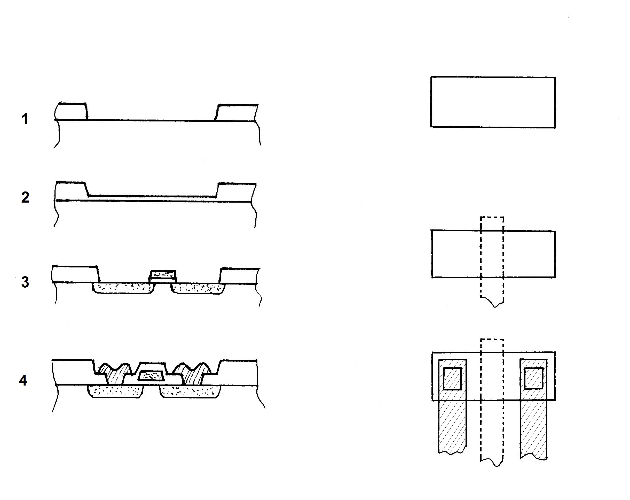
Fig. A1 - The architecture of the MOS process with the silicon gate. Illustration by F. Faggin.
Here we can see clearly why the process is called self-aligned: a misalignment between the tub and the silicon mask would slightly change the geometries of the source and the drain, leaving unchanged all the parasitic capacitances between source, drain, and the gate.
With the metal gate, the impossibility to make a perfect alignment between the first and the second mask requires a larger overlapping area between the gate mask and the source and drain mask, substantially increasing the parasitic capacitances and reducing the speed of the transistors, especially in the worst-case misalignment (Fig A2).
One might ask: How come the process I just described cannot be performed with aluminum instead of silicon? The reason is simple. After depositing the aluminum, the wafer temperature cannot rise above 570°C without damaging the circuits. The process steps that follow, however, require temperatures up to 900°C which only silicon and other possible refractory materials could withstand without problems [5].
The architecture of the MOS aluminum-gate process
To better understand the differences between metal-gate and silicon-gate technologies, figure A-2 illustrates the processing steps with aluminum gate:
- As always, we start with a thick field-oxide layer to which the source and drain mask is applied and the oxide is etched (Fig. A2-1 at left). At the top right of figure A2, the source and drain mask is shown.
- Boron is deposited in the exposed silicon areas (Fig. A2-2 at left).
- An oxide layer is thermally grown. The gate mask is applied and the oxide is removed in the gate area. The gate mask is shown in the second figure at the top right of figure A2 with dotted lines.
- The gate oxide is thermally grown at high temperature and simultaneously the junctions diffuse into the silicon. At the end of this processing step, the structure of the transistor is shown in Figure A2-3 at the left.
- The contact mask is applied to remove the oxide in the areas where the aluminum will make ohmic contact with the junctions. The contact mask is shown in the third figure from the top at right (two small rectangles).
- An aluminum film is vacuum-deposited and the aluminum mask is applied to define the metal lines. The metal mask is shown in the third figure from the top at right (three dashed strips).
- The remainder of the process is identical to the one described above for the SGT and the final structure of the transistor is shown in Figure A2-4.
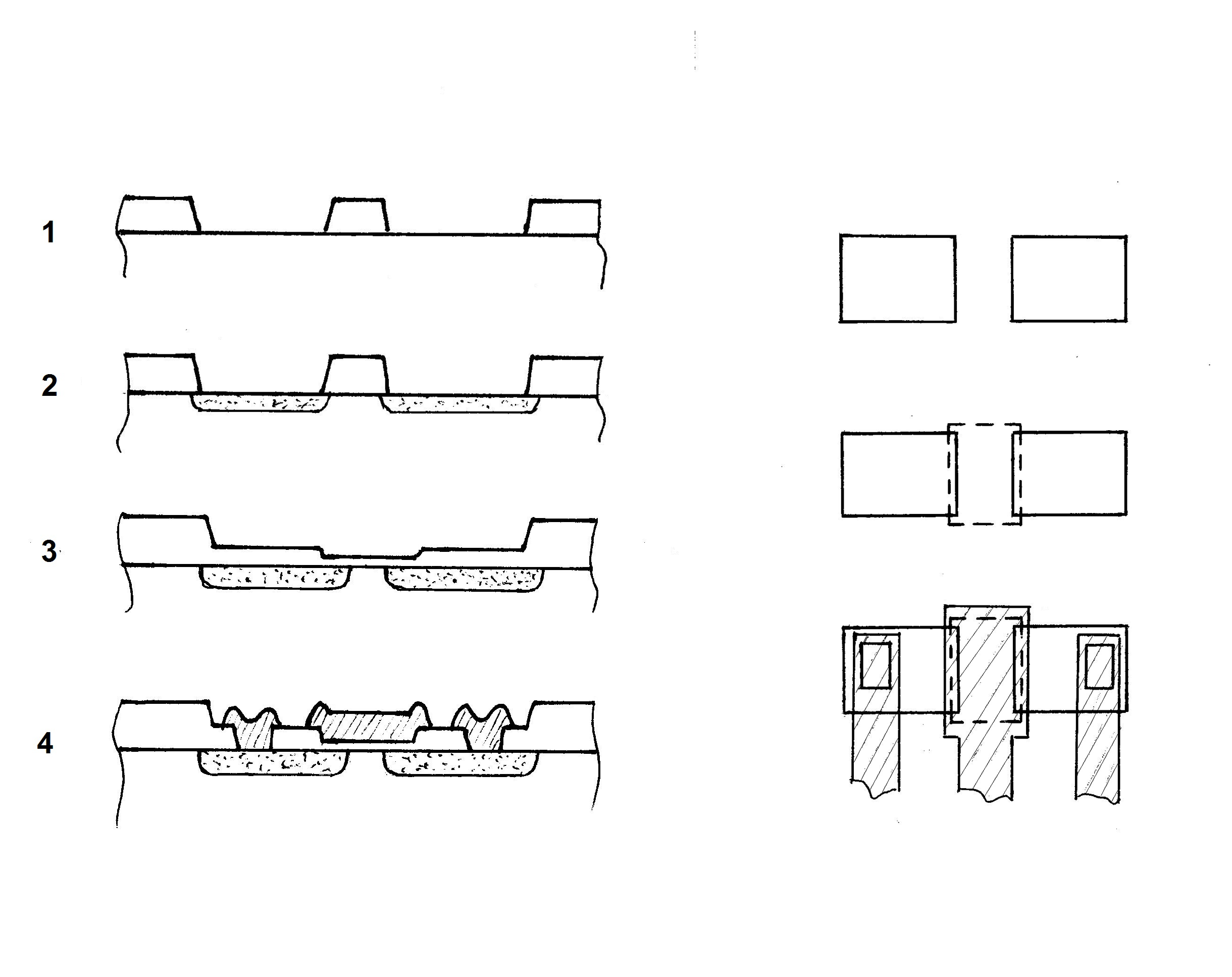
Fig. A2 - The architecture of the MOS process with an aluminum gate. Illustration by F. Faggin
In comparing figure A1-4 with figure A2-4, notice that the overlapping areas between the gate and the source and drain are much larger for the aluminum gate than for the silicon gate. In the case of perfect alignment, the parasitic capacitance of the aluminum-gate transistor is 2.5 times larger than the one with the SGT. In the worst-case misalignment, it is about four times worse. Notice also that the aluminum covers most of the area, increasing the area occupied by the transistor.
The SGT with the buried contact
The variant of the SGT process with the buried contacts requires the removal of the thin oxide in the tub areas where direct contact between the polycrystalline silicon and the single crystal silicon are desired. This requires an additional masking step. The solid line square shown in the upper part of figure A3 represents the buried contact mask.
After the etching of the gate oxide in the contact area, the process continues exactly as described in figure A1.
During the doping process, the boron atoms diffuse through the thin layer of polycrystalline silicon, continue to diffuse into the monocrystalline silicon and form a junction in the contact area. In this fashion, an isolated contact is created which is subsequently passivated with oxide, allowing aluminum lines to cross over it.
The bottom part of the figure shows a cross section of the buried contact area along the cut line AA shown on the top of the figure. Notice the layer of oxide that exists between the aluminum and the polysilicon that provides insulation.
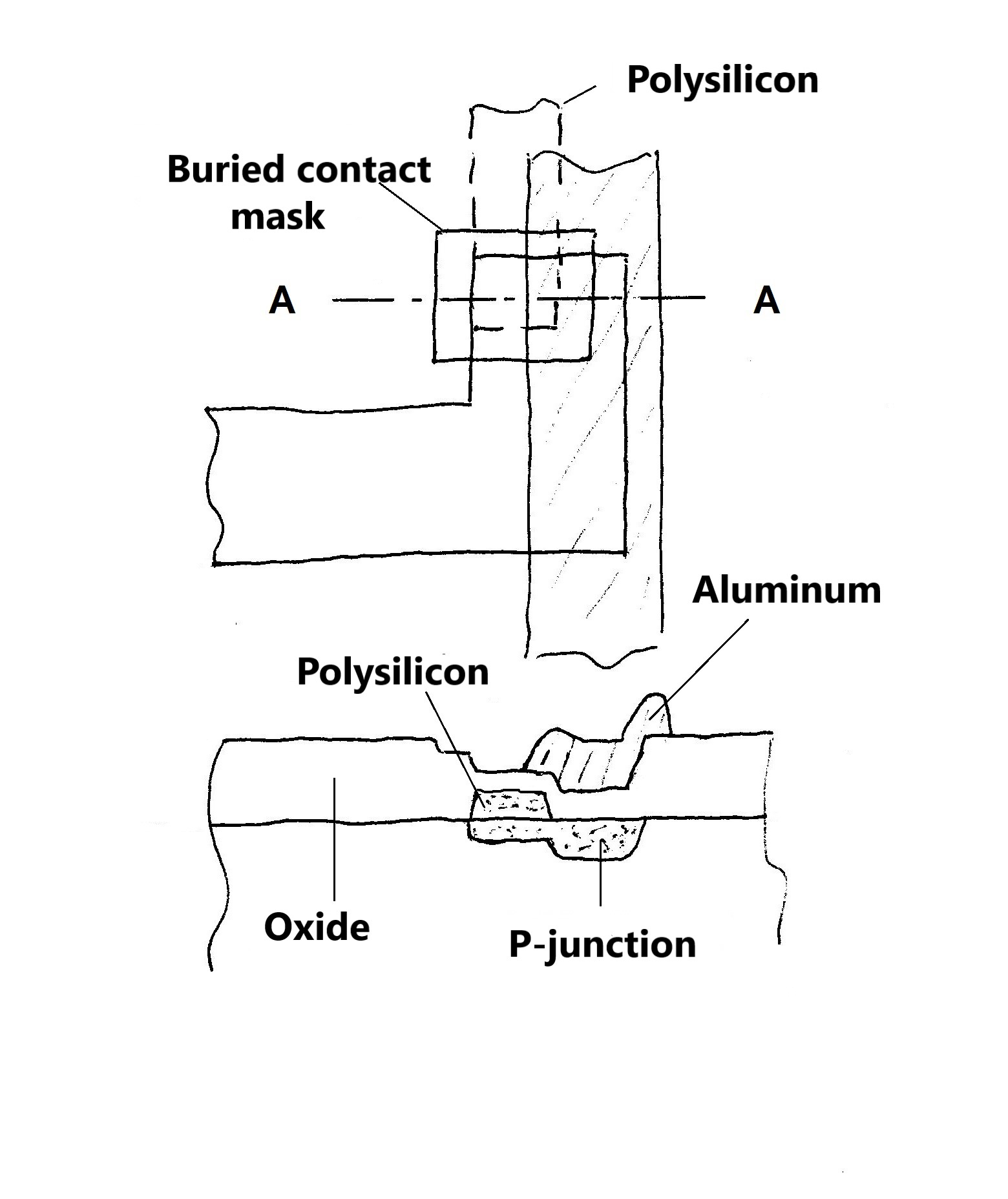
Fig. A3 - This figure shows the layout of the buried contact on the top. The bottom figure shows a cross section of the silicon along the line AA. The solid-line square surrounding the overlapping area between the tub mask (solid line) and the polysilicon mask (dashed line) is the buried-contact mask used to eliminate the thin oxide, thus allowing the polysilicon to be in direct contact with the single-crystal silicon. The boron doping that follows allows the junction to form into the single-crystal silicon as seen in the lower section. Illustration by F. Faggin.
The layout with the SGT
In figure A4 I have recreated one of the examples given to the IC designers of the MOS division to demonstrate the superiority of the SGT in making the layout of random logic circuits, especially if they had used buried contacts. The great advantage of the SGT is obvious.
In the aluminum-gate layout at left, the gates of the transistors (where the oxide is thin), are the areas enclosed by gray dotted-line rectangles. Aluminum is represented by dashed strips. P-doped diffusions, which are used for the sources, drains, and signals crossing under the aluminum, use solid lines. The contact areas between the diffusions and the aluminum are gray rectangles where metal strips and junctions overlap.
In the silicon-gate layout at right, I used the same conventions except for the polysilicon mask that uses gray dotted lines. In this case, the gates of the transistors are the areas of overlap between the tub mask (solid line) and the polysilicon mask.
It is important to note that the parasitic capacitances of the silicon lines used for interconnections were many times lower than those of the diffusions. This further contributed to the greater speed and the layout flexibility of the SGT circuits. With the metal-gate technology, diffusions were the only alternative interconnection layer that could cross the aluminum lines.
In figure A4 on the right, under the aluminum line called S1, there is a buried contact connecting the diffusion corresponding to the output O with a silicon line that becomes the gate of another transistor (not shown in the figure). Naturally, the output O could also cross under the aluminum as a diffusion, exactly like in the case of the metal gate.
I used a buried contact to show the speed advantage offered by the SGT because the silicon output makes the circuit faster than the diffusion output even though the circuit size is unaffected in this case. In most other cases, the buried contact is essential to obtaining a denser layout.
The fundamental advantage of the buried contact is to enable going from diffusion to polysilicon directly, without using aluminum. Aluminum signals can then cross the buried contacts, thus increasing the circuit density and speed.
.jpg.png)
Fig. A4 - On the left is the layout of a NAND logic gate with three inputs: A, B, and C and with output, O, made with aluminum gate. There are also four signals: S1, S2, S3, and S4 that must traverse the circuit, a typical situation for a random-logic integrated circuit. On the right is the layout of the same circuit made with the SGT. The area used in the metal-gate version is almost twice the one used with SGT. The speed of the SGT circuit is five times higher than that with the aluminum gate. Since the production cost is proportional to the area, the advantage of SGT is not only in performance but also in cost. Illustration by F. Faggin.
The bootstrap load
The bootstrap load allowed obtaining an output voltage equal to the supply voltage in a dynamic logic gate, enhancing an efficient and widely used design technique called two- phase dynamic logic. This technique was also called quasi-static logic because one could mix static with dynamic logic circuits.
Let’s consider the case of an inverter with a normal load and with a supply voltage of -15 volts as shown on the left of figure A5. When the transistor T1 is turned off, the output Out is typically about -10 volts (from -8 to -11.5 volts, with process variations). When T1 is on, Out is typically at -0.5 volts.
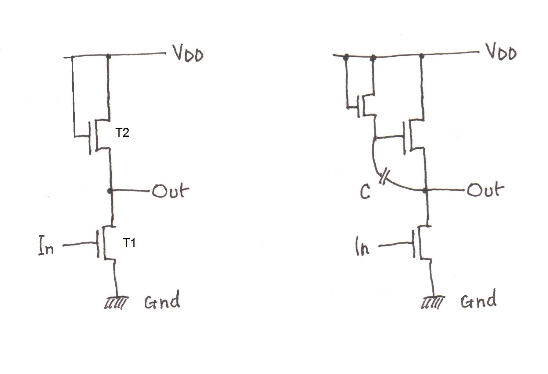
Fig. A5 - Circuit diagram of an inverter with the normal load (figure on the left) and with boot- strap load (figure on the right). Illustration by F. Faggin.
Now consider an inverter with a bootstrap load shown on the right of figure A5. When the input voltage (In) goes from -10 volts to 0.5 volts, the output voltage (Out) goes from -0.5 volts to -10 volts. The capacitor C causes the voltage at node B, which is normally at about -10 volts, to become more negative, completely turning off transistor T3.
A negative change in the output voltage of one volt leads to about a change of -0.8 volts at node B (the value depends on the ratio between the parasitic capacitance of node B and the capacitance C of the bootstrap). Therefore, the voltage at node B continues to decrease in line with the output voltage, keeping the transistor T2 on, even when the output voltage reaches -10 volts at which time the voltage at node B will be -10.8 volts. When the output voltage reaches the supply voltage, node B will be at about -22 volts.
To make a bootstrap load physically, an isolated capacitor was needed. This was trivial to do with metal-gate technology, but impossible with silicon gate since the polysilicon prevents a junction to form under the thin oxide.
No one thought it was possible to make a bootstrap load with silicon gate, myself included. But I did not surrender to the evidence of reasoning that turned out to be only partly correct. I kept thinking about how I could circumvent the problem.
One day I noticed that the metal electrode of the capacitor in the metal-gate bootstrap load was always polarized to keep an inversion layer in the silicon below if I assumed that the diffusion under the thin oxide had been removed (counterfactual thinking). In other words, the operating conditions of the bootstrap load were such that there would always be a "virtual diffusion" under the polysilicon. Therefore, I could have an equally effective capacitor even without a real diffusion! All that was needed was to create a large polysilicon area inside a large tub without obstructing the passage from the drain of transistor T1 to the source of transistor T2, as shown in figure A6.
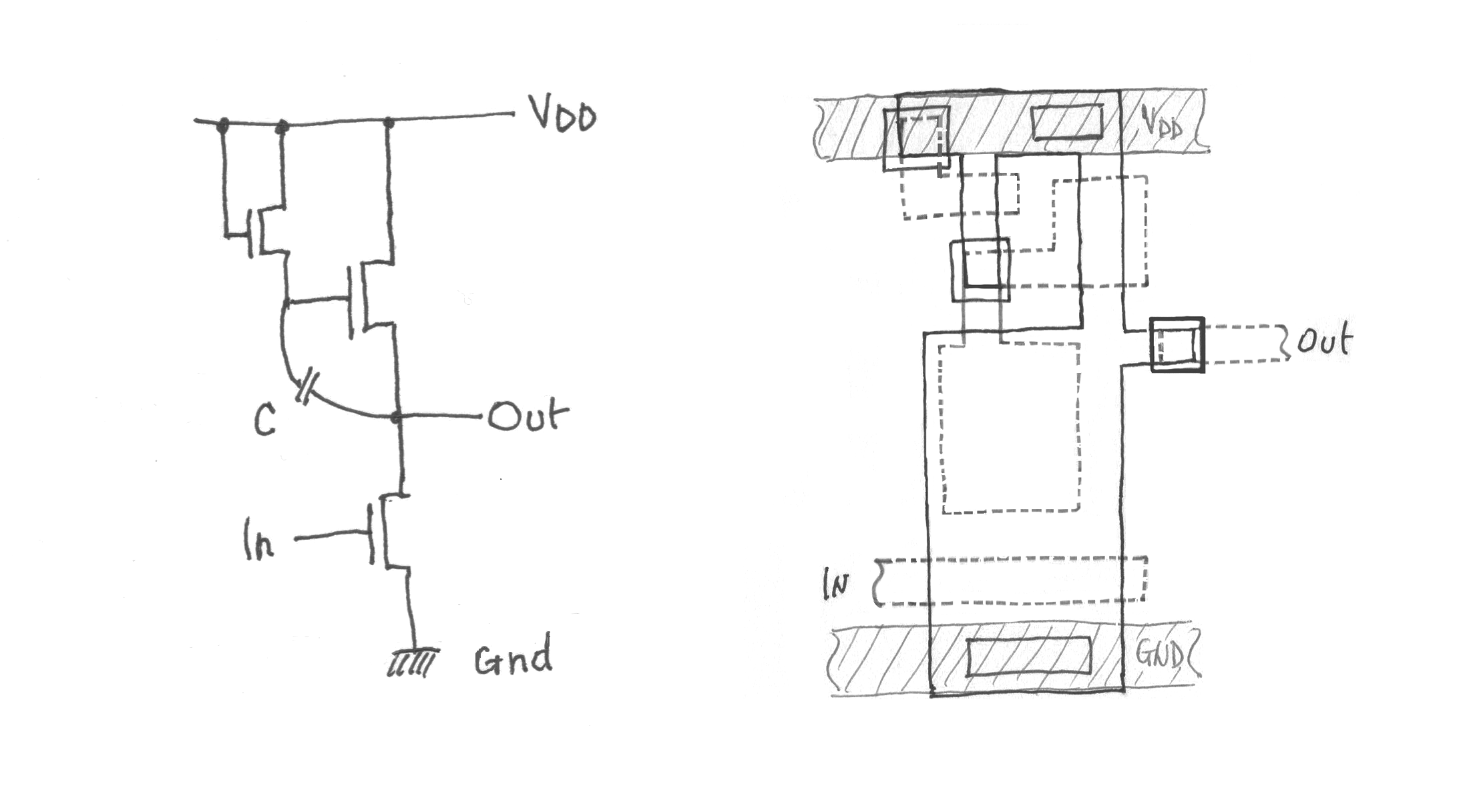
Fig. A6 - The circuit diagram of the bootstrap load is shown on the left. On the right is the layout of the same circuit using the SGT. The capacitor is the large polysilicon rectangle inside the tub which also acts as a drain of the transistor T1. Note the three buried contacts that allow this circuit to be completely "crossable" by other metal lines, a huge advantage since with the metal-gate technology the same circuit would be completely uncrossable by other aluminum lines. Illustration by F. Faggin.
The pass transistor
To make a quasi-static circuit we used a pass transistor, the gate of which was typically driven by a logic gate as shown by the node A in figure A7. The drain of the pass transistor was connected to the output B of a logic gate and the source was connected to the gate of another transistor (node C).
The great advantage of a MOS transistor was the ability to temporarily store a charge (information) in the capacitance of the gate of a transistor, like the node C, after the pass transistor had been deactivated.
Fig. A7 - Example of a random-logic circuit where the gate of a pass transistor must be driven by a logic port with a bootstrap load to work. Illustration by F. Faggin.
The worst-case output signal produced by a logic gate with a normal load was -8 volts. If this signal had been applied to the gate of a pass transistor, the output voltage of the latter would have been about -4 volts, slightly higher than the worst-case threshold voltage of a transistor (-3.5 volts). This condition would render unusable the precious function of a pass transistor.
To take advantage of the information storage allowed by the pass transistors it was necessary to use a bootstrap load in the logic gate that controlled the transistor as shown in figure A7.
This "trick" allowed for drastically reducing the number of transistors needed to make a dynamic MOS logic circuit, compared to a static circuit. It was also the main reason why MOS technology required far fewer transistors than bipolar to make the same logical function. For example, with a pass transistor, it was possible to realize a dynamic flip-flop with only three transistors, while a static MOS flip-flop would require a minimum of six and a bipolar flip-flop more than 15. Without the bootstrap load, the only alternative was to use static logic circuits that required many more transistors and far greater power dissipation for the same speed.
Push-pull buffers
Another essential circuit that required bootstrap loads was the push-pull buffer. Buffers were needed whenever a logic gate had to drive a large capacitive load without dissipating excessive power. For example, these buffers were indispensable in complex logic circuits to drive internal buses.
A push-pull buffer is shown in figure A8. When IN has a logic value “0," the transistors T1 and T2 are off, node A is at logic value "1" and therefore T3 is on.
When IN has a logic value "1" the transistors T1 and T2 are on and node A is at logic value "0." In this case, T3 is off.
Therefore, when T2 is on, T3 is off and vice versa. This allows both T2 and T3 to be large transistors capable of driving large capacitive loads, impossible to do if T2 and T3 were both on as it occurs in a normal inverter.
The bootstrap load is necessary to drive T3, otherwise, the output voltage (OUT) would be -4 volts, in the worst-case, instead of -8 volts, the minimum voltage required for the logical value “1."
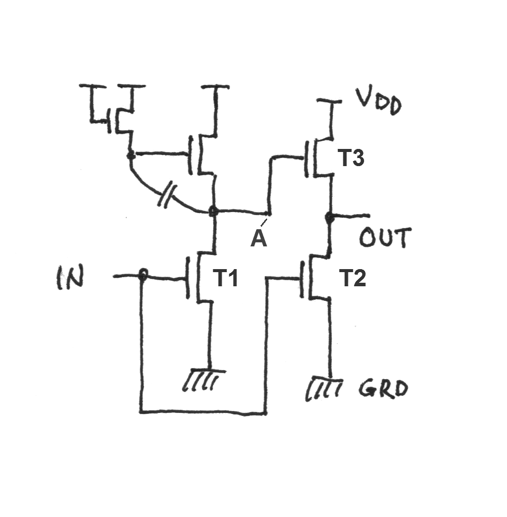
Fig. A8 - Push-pull buffer. The bootstrap load is necessary for the same reason discussed in the case of the pass transistor. Without the bootstrap load, the output voltage (OUT) would be -4 volts (in the worst-case) instead of -8 volts, the minimum voltage required for the logical value “1.” Illustration by F. Faggin.
The depletion load
Consider an N-channel transistor in which the starting material is a P-type wafer and the source and drain junctions are N-doped. This device has a positive threshold voltage and the supply voltage VDD is also positive. In the following description, we assume that VDD is 5 volts. For conduction to occur, a voltage more positive than the threshold voltage must be applied to the gate of the transistor. When the gate is at zero volts, the transistor is off (does not conduct). A transistor that is off when its gate voltage is at the same potential as its source is called enhancement mode.
Surprisingly, it is also possible to fabricate N-channel transistors which are normally on when its gate is at the same potential as its source. This type of transistor is called depletion mode.
To fabricate a depletion-mode transistor it is necessary to create a weak N-channel at the interface between the silicon and the gate oxide using arsenic ion implantation (type N). The result is a transistor with a negative threshold voltage instead of a positive one, making it always conducting for the normal positive voltages available in an N-channel integrated circuit.
To turn the transistor off, a negative voltage larger than its threshold voltage would be required — a voltage unavailable in a chip with only a +5-volt supply voltage. This property would make a depletion-mode transistor useless for normal applications. However, if it were used as a load device to replace a normal enhancement-mode transistor, this property would be priceless. Let’s see why.
Figure A9 shows how the load current (I) varies with the variation of the output voltage (V) for a normal enhancement load and a depletion load when the two loads are sized to have the same maximum current (IM) and therefore the same power dissipation.
With normal load, the output voltage is VDD – VT, which in the worst-case is about 2.5 volts, a value about 1 volt higher than the maximum threshold voltage of an enhancement transistor. With the depletion load, the output voltage is 5 volts, equal to the supply voltage. The speed of the load when driving the gate of another transistor is proportional to the area marked with a double line in the case of the normal load and the area marked with a single line in the case of the depletion load. The clear superiority of the depletion load can be immediately appreciated by the figure.
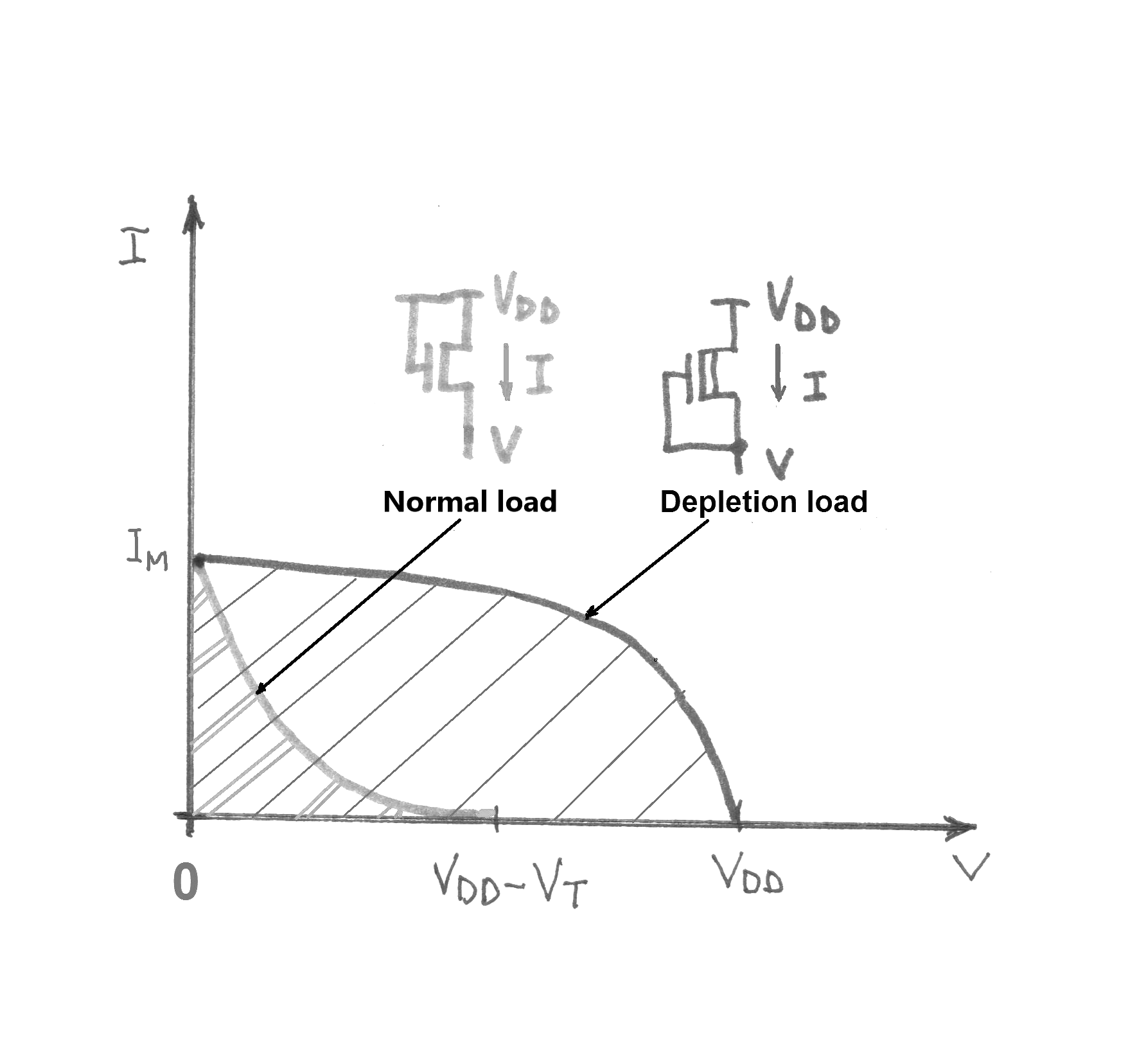
Fig. A9 - The characteristics of normal load and depletion load. Illustration by F. Faggin.
A depletion load behaves like a bootstrap load to obtain an output voltage equal to the supply voltage, with the additional advantage of being static rather than a dynamic circuit. N-Channel technology with depletion load made it possible in 1973-1974 to design fast integrated circuits with a supply voltage of only 5 volts, the standard supply voltage used in all bipolar logic circuits. This technology was universally used for 10 to 15 years before being superseded by CMOS technology, the dominant technology today.
Note 1 – A parasitic MOS transistor is an unintentional device obtained when a metal line over the field oxide crosses two junctions. In this case, the junctions act like the source and the drain of a parasitic MOS transistor and the metal line acts as its gate. If the voltage of the metal line is higher than the threshold voltage of the parasitic MOS in which the field oxide is the “gate oxide,” an inversion layer is created in the underlying silicon leading to a weak electrical connection between the two junctions that should be isolated. A parasitic transistor is particularly damaging in the case of dynamic circuits because the information temporarily stored as an electric charge in the gate of a transistor could rapidly leak away, causing a malfunction.
Note 2 – The metal thinning at the oxide step, due to the vacuum evaporation of aluminum, not only causes yield problems, but it could also create serious reliability problems in the field due to electromigration. Electromigration causes the aluminum interconnections to thin down and open (over time) if the current density exceeds a certain limit